
热门标签
热门文章
- 1华硕ROG品牌机安装ubuntu双系统_华硕rog魔霸7plus装ubuntu
- 2linux版本i686,linux-x86_64平台上的gcc i686
- 3基于TF-IDF代码实战:文本实体关系抽取 有代码数据可直接运行_视觉文档关系提取代码
- 4with torch.no_grad() 和 叶子节点in place操作_叶子节点可以进行inplace操作吗
- 5openGauss安全加固指南:账号口令管理_opengauss 密码过期
- 6使用Navicat一次性导入多个数据表_navicat批量导入多个文件
- 7STM32电调控制无感无刷电机_stm32控制电调
- 8检测任务评估指标AP和AR_ar ap
- 9超牛无损图片放大神器PhotoZoom_超牛损放大软件
- 10RabbitMQ实战知识详细笔记,消息丢失,重复消费等问题解决方案。_rabbitmq一个队列里的其中一个事件一直在消费怎么调查
当前位置: article > 正文
Vivado综合属性之ASYNC_REG_vivado中的cdc
作者:木道寻08 | 2024-08-11 07:50:42
赞
踩
vivado中的cdc
本文验证了综合属性ASYNC_REG对寄存器位置的影响。
ASYNC_REG用于单bit信号采用双(或多)触发器实现异步跨时钟域的场合,此时所有用于同步的触发器都要标记ASYNC_REG。标记方式为:
(* ASYNC_REG = "TRUE" *) reg sync_0, sync_1;
目的是告诉综合工具布线时将这2个寄存器放在一起(即同一个SLICE中),从而减少线延迟对时序的影响。
为避免忘记标记ASYNC_REG,打开Language template -> XPM_CDC -> Single-bit Synchronizer(xpm_cdc_single),见下方代码:
- xpm_cdc_single #(
- .DEST_SYNC_FF(4), // DECIMAL; range: 2-10
- .INIT_SYNC_FF(0), // DECIMAL; 0=disable simulation init values, 1=enable simulation init values
- .SIM_ASSERT_CHK(0), // DECIMAL; 0=disable simulation messages, 1=enable simulation messages
- .SRC_INPUT_REG(1) // DECIMAL; 0=do not register input, 1=register input
- )
- xpm_cdc_single_inst (
- .dest_out(dest_out), // 1-bit output: src_in synchronized to the destination clock domain. This output is
- // registered.
-
- .dest_clk(dest_clk), // 1-bit input: Clock signal for the destination clock domain.
- .src_clk(src_clk), // 1-bit input: optional; required when SRC_INPUT_REG = 1
- .src_in(src_in) // 1-bit input: Input signal to be synchronized to dest_clk domain.
- );
创建top.v,代码如下:
- module top(
- input src_clk,
- input src_in,
- input dest_clk,
- output dest_out
- );
- xpm_cdc_single #(
- .DEST_SYNC_FF(2), // DECIMAL; range: 2-10
- .INIT_SYNC_FF(0), // DECIMAL; 0=disable simulation init values, 1=enable simulation init values
- .SIM_ASSERT_CHK(0), // DECIMAL; 0=disable simulation messages, 1=enable simulation messages
- .SRC_INPUT_REG(1) // DECIMAL; 0=do not register input, 1=register input
- )
- xpm_cdc_single_inst (
- .dest_out(dest_out), // 1-bit output: src_in synchronized to the destination clock domain. This output is
- // registered.
-
- .dest_clk(dest_clk), // 1-bit input: Clock signal for the destination clock domain.
- .src_clk(src_clk), // 1-bit input: optional; required when SRC_INPUT_REG = 1
- .src_in(src_in) // 1-bit input: Input signal to be synchronized to dest_clk domain.
- );
- endmodule
在Open Implemented Design -> Schematic中的原理图(不是综合后的原理图)为:
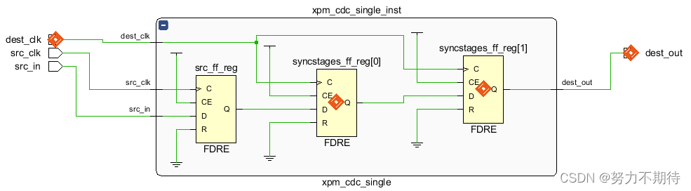
上图将dest_clk连接的2个FF MARK了,对应到Device界面的视图如下:
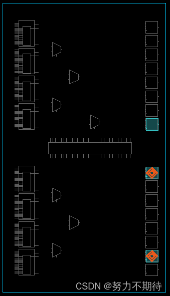
上图淡蓝色括住的表示一个SLICE,红色MARK对应上上图的2个寄存器FDRE,可以看出它们是在一个SLICE中的。
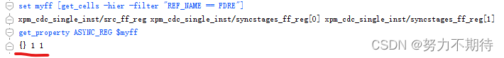
通过如下代码可验证ASYNC_REG是否已被标记:
- set myff [get_cells -hier -filter “REF_NAME == FDRE”]
-
- get_property ASYNC_REG $myff
执行结果如下时说明ASYNC_REG是否已被标记:

声明:本文内容由网友自发贡献,不代表【wpsshop博客】立场,版权归原作者所有,本站不承担相应法律责任。如您发现有侵权的内容,请联系我们。转载请注明出处:https://www.wpsshop.cn/w/木道寻08/article/detail/963019
推荐阅读
相关标签

